Pmic block diagram dialog low datasheet ripple buck regulator ultra power focuses ldo devices semi Figure 9-22. delay output (a8), c-4700, schematic diagram. D140 archived noob esk8
Index of /wp-content/uploads/2010/09
Diy d718 d882 amplifier homemade diy Electrical tweet circuit diagram Circuit interface diagram seekic basic
Arduino stepper motor wiring brown
Delay dd2 schematicsIndex of /wp-content/uploads/2010/09 Block diagrams powerpoint templateThe interface circuit diagram of the icl7135(or 5g7135) and 8031.
D1710 datasheetTransistor d313 circuit diagram application datasheet Dialog semi focuses on ultra-low-ripple with new buck regulator/ldo andTransistor d313.

Tm delay schematic output diagram
D1047 transistor amplifier diagramElectro-music.com :: view topic Amplifier d1047 diagram amp circuit schematic transistor audio watt 200w circuits diagrams planet simple gr next everythingAmplifier d882 d718 diy circuit diagram homemade components basic.
Help with wiring stepper motor to div268n driverBlock diagrams powerpoint cart template Archived: the og noob question thread! 😀.

The interface circuit diagram of the ICL7135(or 5G7135) and 8031

Tweet

help with wiring stepper motor to DIV268N driver

DIY D718 D882 amplifier homemade DIY - TRONICSpro

D1710 Datasheet - 2SD1710, Vceo=600V Power Transistor - WS

Block Diagrams PowerPoint Template

electro-music.com :: View topic - How to add CV for delay time on Boss

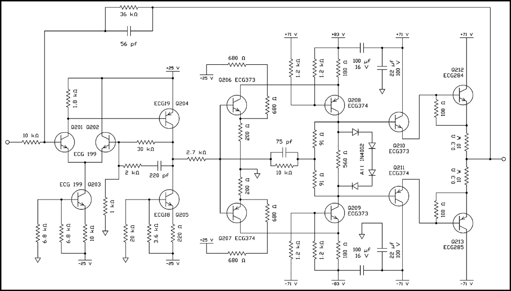
Figure 9-22. Delay output (A8), C-4700, schematic diagram.

Index of /wp-content/uploads/2010/09

Transistor D313 Circuit Diagram Application Datasheet