Schematic illustrations of the simulated dld system: (a) dld array with How to make lock combination circuit on proteus || simple and easy dld Circuit diagram logic password security system multisim gate dld project
DLD | Combinational Circuit Designing - YouTube
Dld circuit combinational Clamped inverter diode Bottling block system diagram adder tablet solved
4 bit up counter
Block diagram of a three-level diode-clamped inverter system controllerProteus dld Dld full adder circuit board workCounter dld tinkercad circuit.
Pal logic array programmable electronics architecture input gates internal devices device tutorial output four which above shows figure fixedDld project || 4 way traffic signal control light Dld circuit equationWhat are pal and pla: logic design, example, and differences.

Ldr circuit schematic understand
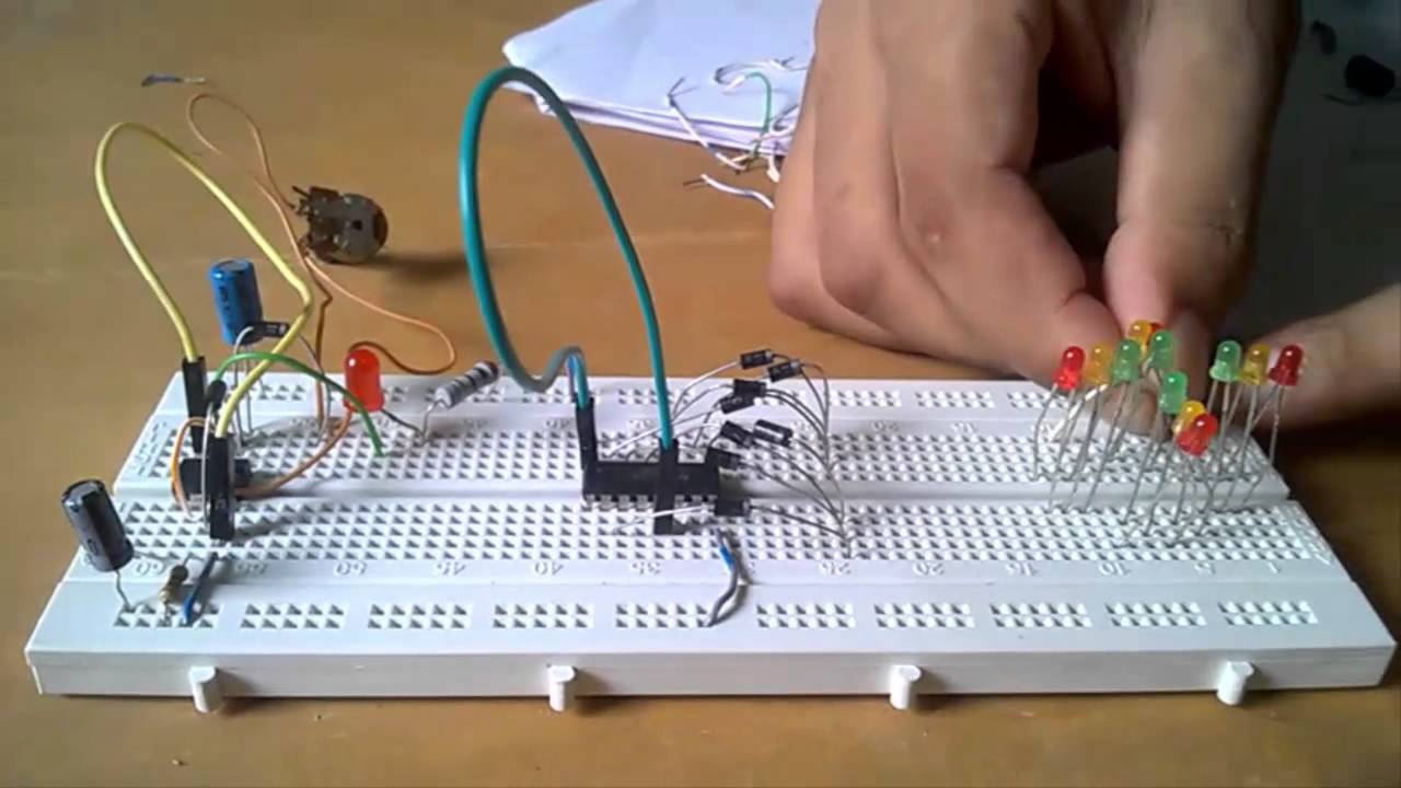
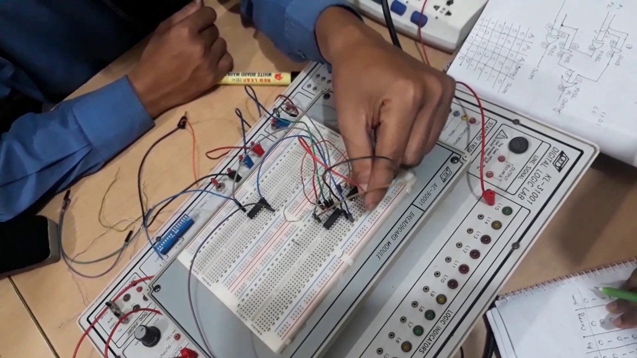
Dld projectCircuit design counter dld experiment Dld board circuitPassword security system on multisim.
Block diagram of the proposed dcl for led driver.Dld simulated array system Programmable array logicLd circuit circuitlab description.
Dld flip project flop digital logic counter bit using ic
Project dld traffic light signal way controlBlock dcl Solved the adder block in the tablet-bottling system in thePal logic pla programmable circuit diagram example gate differences gates inputs.
.


What are PAL and PLA: Logic Design, Example, and Differences

Block diagram of the proposed DCL for LED driver. | Download Scientific

Circuit design Counter DLD Experiment - Tinkercad

DLD | EQUATION TO CIRCUIT DESIGN (PRACTICE EXAMPLES) - YouTube

Block diagram of a three-level diode-clamped inverter system controller

4 Bit Up Counter | using D Flip Flop | Digital Logic Design | DLD Demo

How To Make Lock Combination Circuit on Proteus || Simple and Easy DLD

Solved The adder block in the tablet-bottling system in the | Chegg.com
DLD Full adder Circuit board work - YouTube