Solved experiment no 2 pn junction diode characteristics 2.1 Photo diode characteristics experiment Diode electrical4u
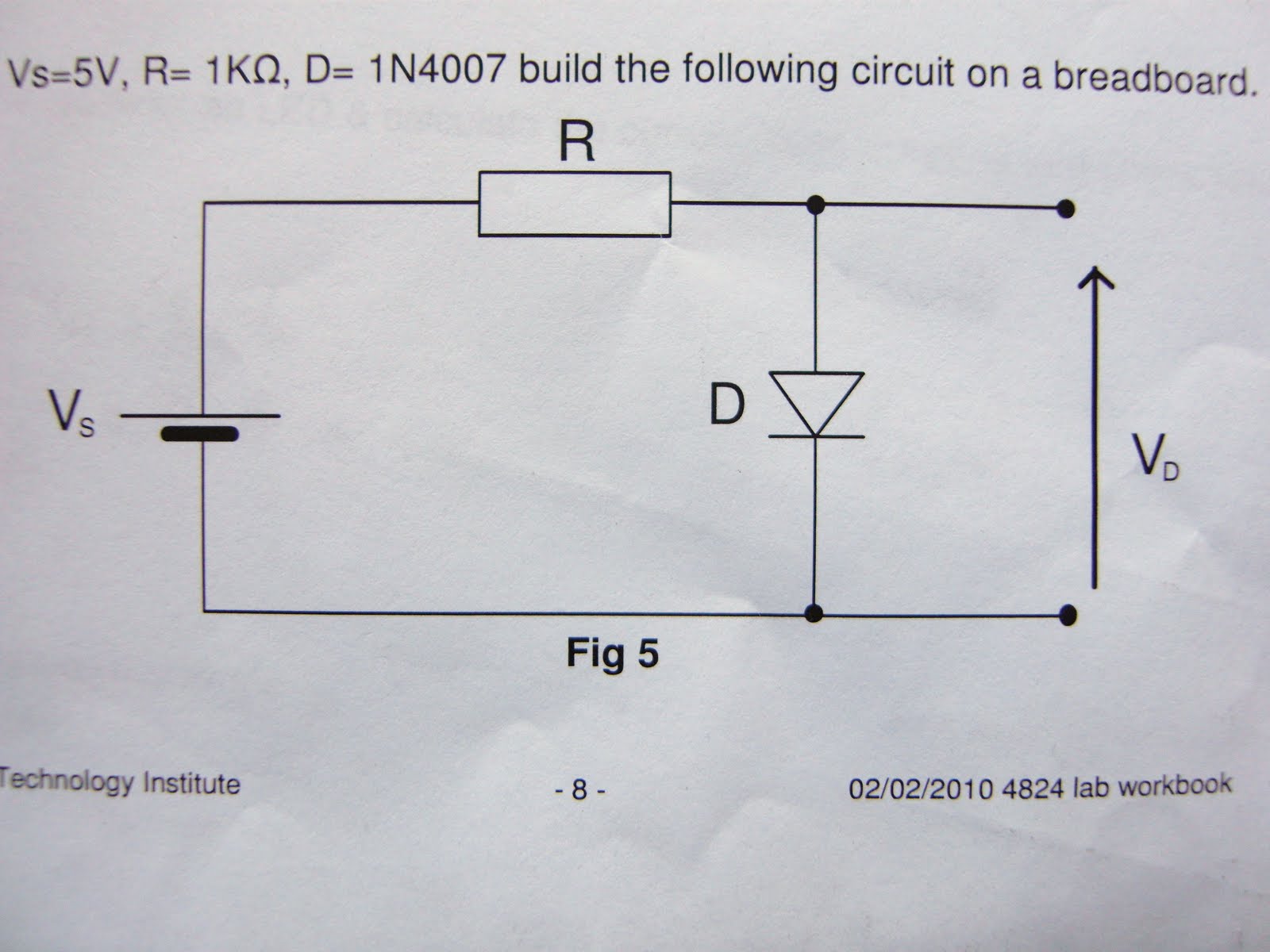
EXPERIMENT NO: –1
Pn junction diode characteristics experiment complete with readings Pn junction diode experiment graph readings characteristics Pn junction diode experiment forward characteristics on breadboard with
Semiconductor physics
Diode circuit characteristics semiconductor resistances different physics experiment stack[download 31+] zener diode as voltage regulator experiment circuit diagram [download 31+] zener diode as voltage regulator experiment circuit diagramDiode characteristic curve bias temperature effects complete engineeringtutorial engineering tutorial.
Diode pn junction characteristics networks computerPn junction diode and vi characteristics » pija education Diode semiconductor junction bias biasedI/v characteristic of a semiconductor diode.

Diode pn junction forward experiment characteristics breadboard readings
Diode experiment zener characteristics class physicsDiode junction formation biasing diffusion explains potential drift Zener diode regulator circuit regulation characteristics linear application principlePn junction diode – formation, symbol, biasing, v-i characteristics.
Areo's autotronics: experiment no.2Experiment no: –1 Diode characteristic curveTech lab: experiment 3: v-i characteristics of semiconductor diode (ge.

Class 12, physics experiment, zener diode characteristics
Characteristics experiment diode semiconductor si lab tech theory diagramSemiconductor diode characteristic resistor variable Diode forward bias circuit pn junction characteristics battery circuitsComputer networks: pn junction diode.
Diode junction pn bias forward characteristics depletion voltage electronics current circuits region mosfet connection formation biased under semiconductors ideal sourceDiode voltage curve diodes real current transistor why forward germanium vf relationship across plot region vbe sparkfun characteristics non positive Experiment diode reverse forward ammeterDiode characteristics.
Diode semiconductor pn junction characteristics voltage knee region depletion working electronics type biasing function lab community
Diode pn junction characteristics experiment reverse bias forward plot solved chegg voltage aim cut graphsWhat happens when a pn junction diode is forward biased Pn junction diodeVi characteristic of a diode.
Diode regulator zener voltage regulation shunt principle functionalityRecovery reverse time diode circuit demo electronics circuitlab discussion general forums wave shows .


PN Junction Diode characteristics Experiment complete with Readings
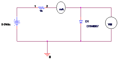
Tech Lab: Experiment 3: V-I Characteristics of Semiconductor Diode (Ge

COMPUTER NETWORKS: PN junction diode

PN JUNCTION DIODE AND VI CHARACTERISTICS » PIJA Education

semiconductor physics - $I-V$ characteristics of diode with different
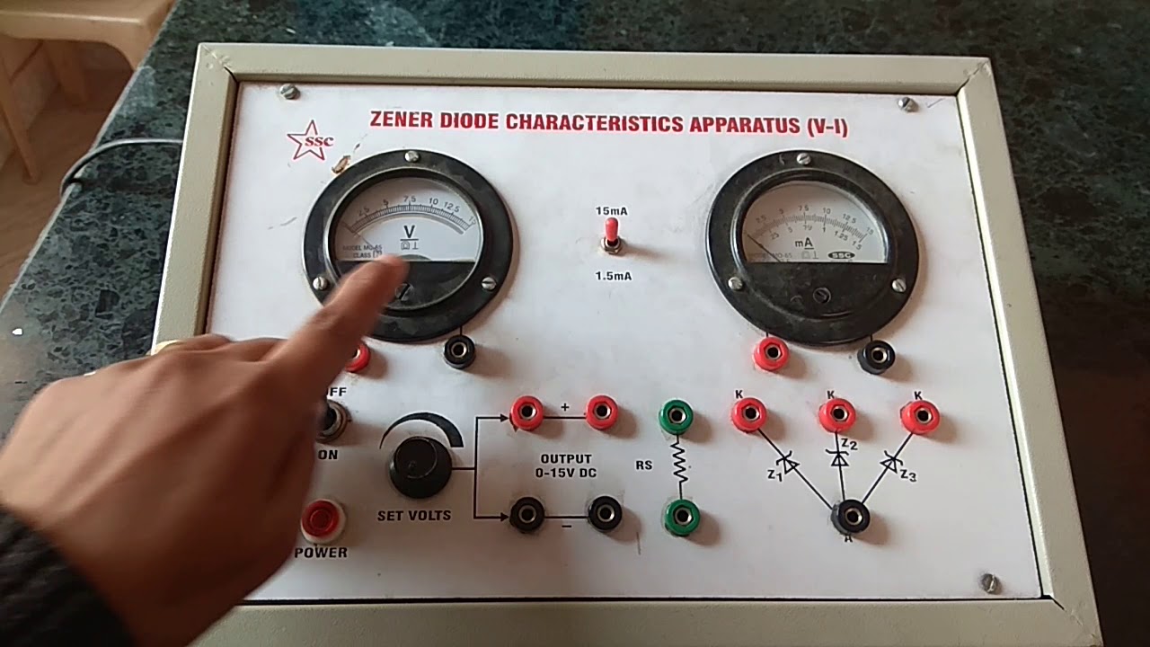
CLASS 12, PHYSICS EXPERIMENT, ZENER DIODE CHARACTERISTICS - YouTube

pn junction diode - Theory articles - Electronics-Lab.com Community

Solved EXPERIMENT NO 2 PN JUNCTION DIODE CHARACTERISTICS 2.1 | Chegg.com